Appendix A: Mifare Classic 101
Since we will be looking at (read as molesting) Mifare Classic I thought it would be fruitful to write up a modest data-sheet type appendix. This way I won't have to keep explaining Mifare internals for each case study and if people have questions I can tell them to RTFM!
I should mention that nxp.com is the authoritative source for information about Mifare internals and if you have your thinking cap on you should read their design specifications. Most of what I will be reviewing here today comes from them and any images in this post have been shamelessly borrowed from their design manuals. I'm doing this with a fair use policy in mind but if anyone has an issue with this feel free to contact me.
This appendix specifically deals with Mifare Classic 1k cards but should generally apply to 4k as well. At the end of the appendix I will add a section that covers the differences between 1k and 4k.
Physical Properties / High Level Overview
Antenna:
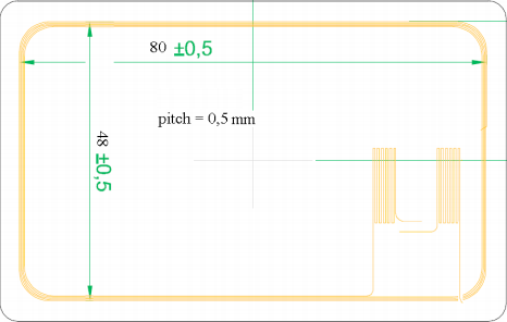
Below you can see the design of the antenna coil for the Mifare card. The antenna is hooked up the to Mifare chip. Any communication is initiated by the reader and controlled by the Digital Control Unite which powers the card's chip. The response will depend on the access conditions for the memory in the corresponding sector.
Anti-Collision:
To avoid conflicts between cards the card UID is read. If multiple cards are in the operating field of the reader they can be told apart by their UID and one single card can be selected for further communication. The other cards will return to an idle state and wait for new commands to be sent. It is worth mentioning that the card UID which is 4-bytes long is non-unique, two Mifare cards can have the same UID (the possible UID's that can exist with 4-bytes have long since been exhausted).
Three Pass Authentication:
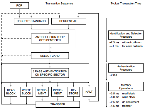
After a Power-On Reset (POR) has been sent by the reader the card will become operational. The reader will then specify which memory it wishes to access and initiate a three pass authentication using the appropriate sector keys. After successful authentication all further communication is encrypted. You can see a graphical representation of the authentication scheme below.
Memory Layout:
The Mifare 1k memory layout is as follows. 1024 x 8 bit EEPROM memory organized into 16 sectors of 4 blocks each. The sectors start at 0 and go up to 15. You can see a graphical representation below. Any images I have found of this depict the sectors in reverse order, I’m not sure why as any dumps I have looked at have been in regular order.
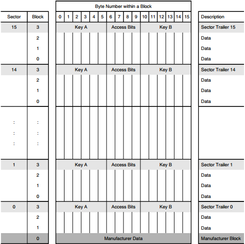
From the image above we can see that the 4th block of each sector is reserved for the sector trailer and the first block of sector 0 is the manufacturer block.
Manufacturer Block:
The manufacturer block contains the Non Unique Identifier (NUID), the 4th byte is a LRC with a rolling XOR and the rest is manufacturer data. This block is write protected at the time of manufacturing.

Sector Trailer:
As mentioned before the sector trailer is always the 4th block of each sector. The sector trailer contains both secret key A&B and access control bytes that dictate what kind of memory operations are allowed on a given sector (read, write, read|write). If key B is not needed the last 6-bytes of the sector trailer can be used as data. Per default blank cards are delivered with all keys set to 0xffffffffffff.

Access Control Bytes:
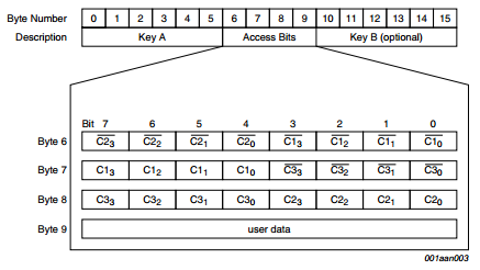
The access control bytes are more than a bit confusing, that’s why half the search queries on google redirect you to a program that "calculates" the access conditions. That is not to say they aren't efficient hehe. As explained each sector is composed of 4 blocks. The first 3 blocks are used for data and the last block is the sector trailer. From the image above, bytes 6-8 are the access control bytes and byte 9 is a general purpose byte.
These three bytes define the access rights for all 4 blocks in the sector including the sector trailer. Each block has 3 bits associated with it. Below you can find 2 tables that define the three bits for respectively the data blocks and the sector trailer block.
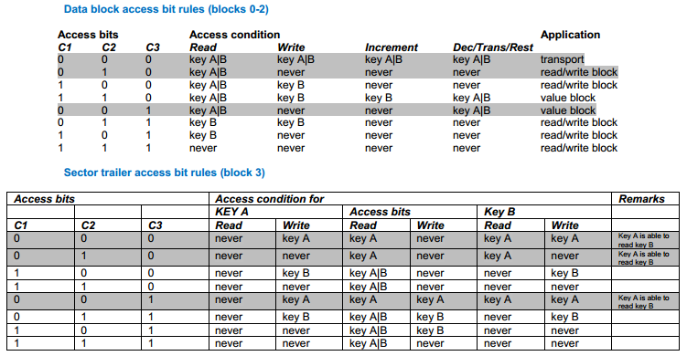
As if that wasn't confusing enough the inverted bit values are also stored, this is done to make sure that the block memory hasn't been corrupted. If the values don't match up the card will assume the memory is corrupt or has been tampered with and will block all access to the whole sector. Below you can see another image that hopefully clears things up a little bit. At the bottom of this appendix I have included a link to a pdf which explains these access control bytes in more detail.
Mifare 4k
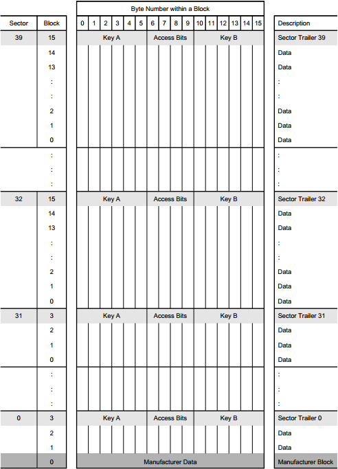
For the most part the Mifare 4k cards are organized in the same way. The only significant difference that will be of importance to us is the added memory and the way that is laid out. The Mifare 4k card has 4096 x 8 bit EEPROM memory that is organized in 32 sectors of 4 blocks and has an additional 8 sectors that contain 16 blocks each. I have included a link to nxp's 4k data-sheet at the bottom of the appendix where you can go over everything in detail. You can see a graphical representation of the Mifare 4k memory layout below.
Reading Material
* Nxp's Mifare classic 1k design specification document. - here
* Nxp's Mifare classic 4k design specification document. - here
* Document by Amal Graafstra describing how the Access Control Bytes work - here
* "Dismantling MIFARE Classic" vulnerability research done by the university of Nijmegen - here
* "Mifare Classic Analysis" vulnerability research done by Nethemba - here
